
PCB laminates
Low DK Laminates 2.0-3.9
Dk and Df determine high-frequency PCB loss, radiation and circuit size. The right material combination balances conductor and dielectric loss against layout dimensions and coupling.
| No. | Image | Product | DK | Df | Detail |
|---|---|---|---|---|---|
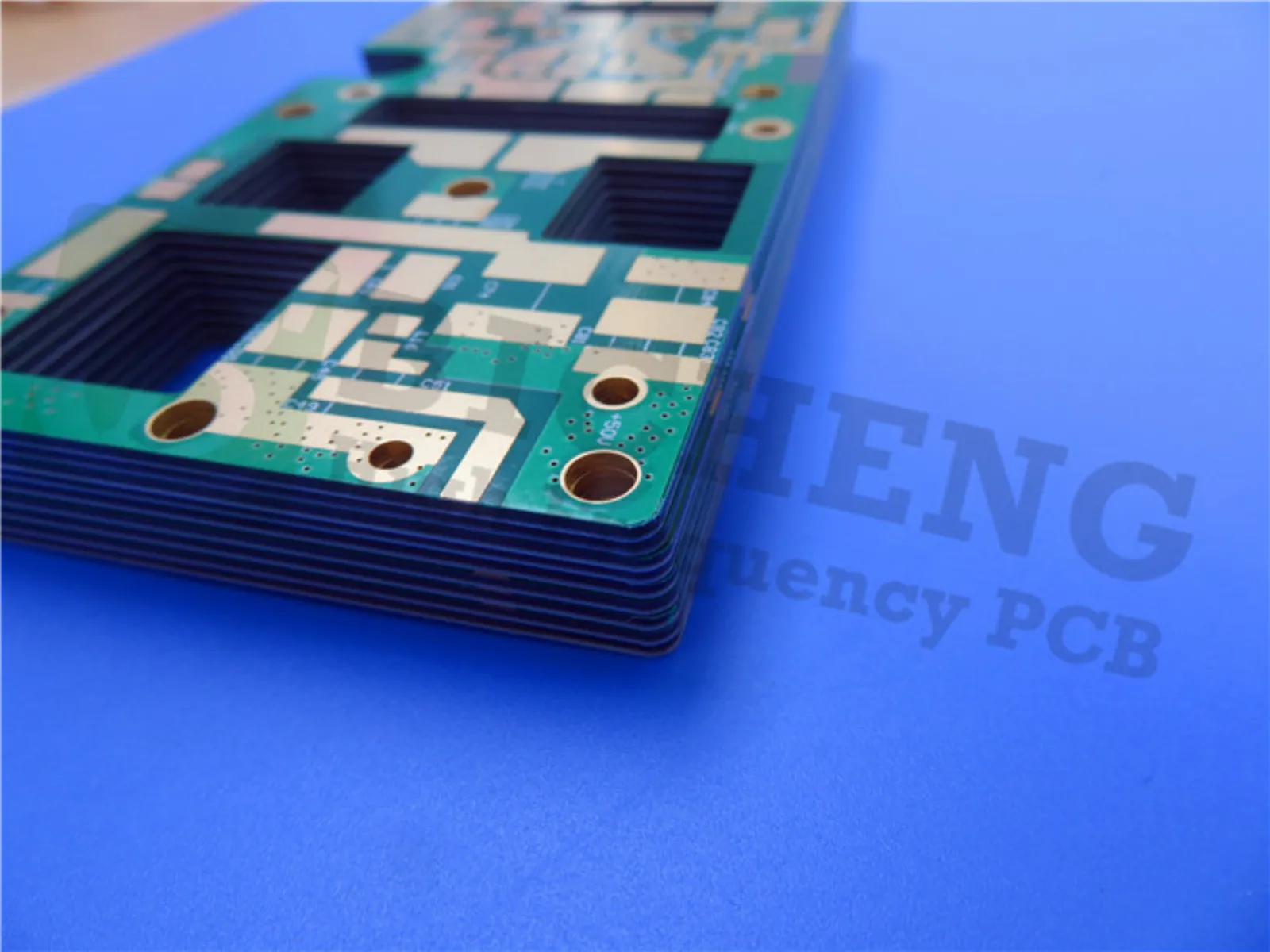 | Rogers RT/duroid 5880LZ LaminateDK 2.00Df 0.0021 | ||||
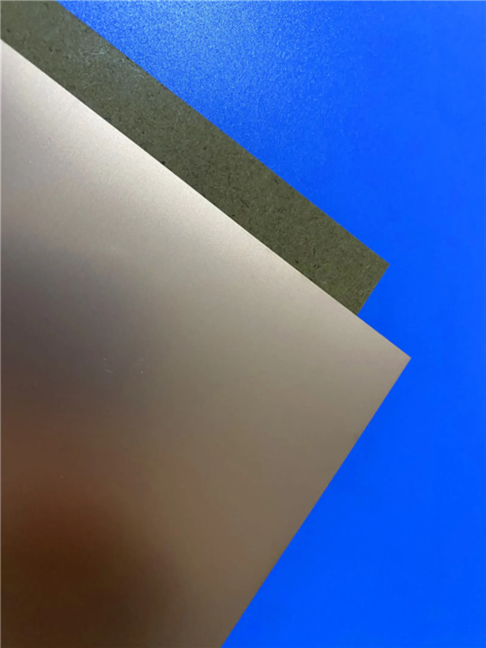 | Rogers CuClad 217 LaminateDK 2.17Df 0.0009 | ||||
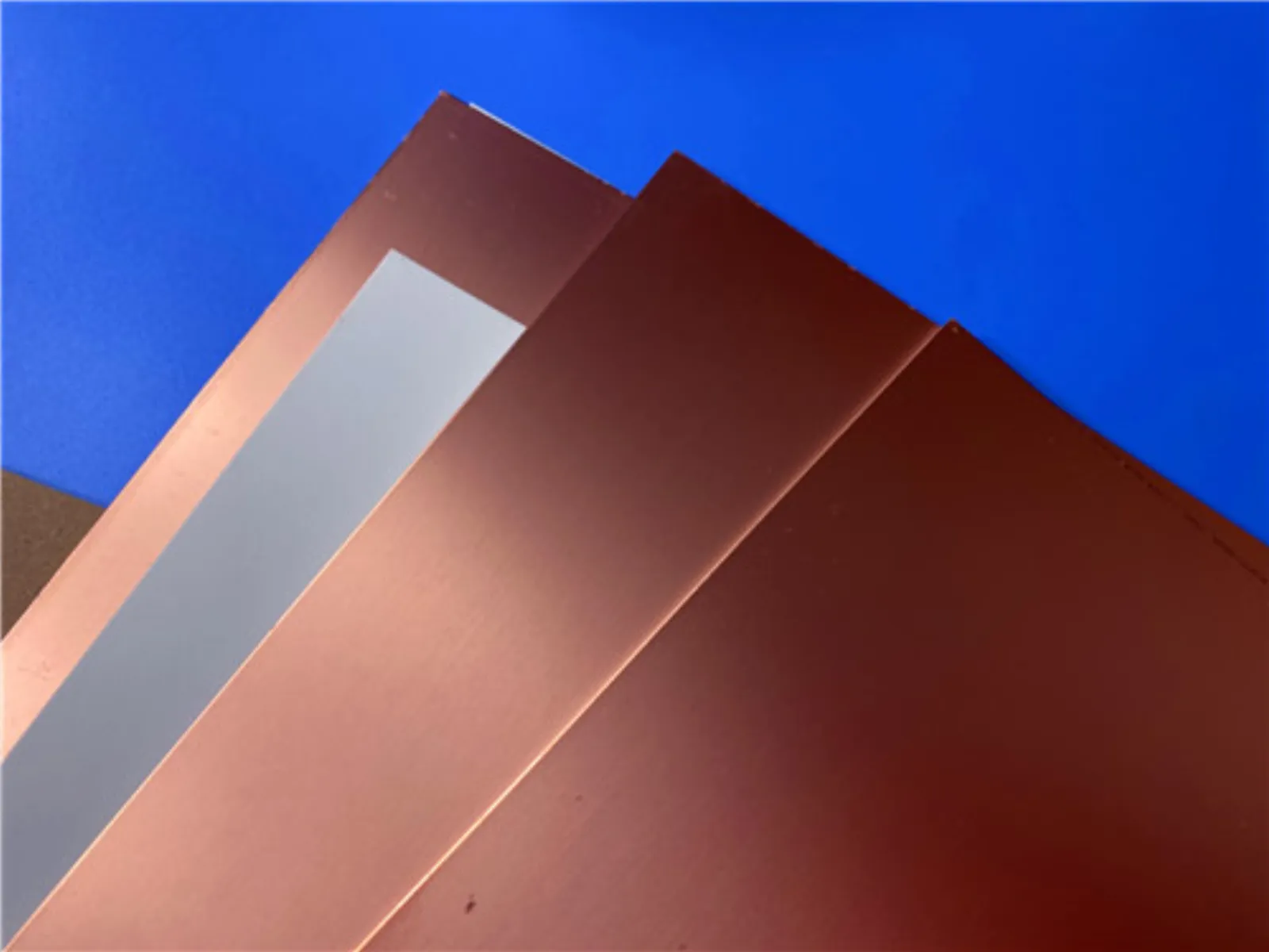 | Rogers DiClad 880 LaminateDK 2.17Df 0.0009 | ||||
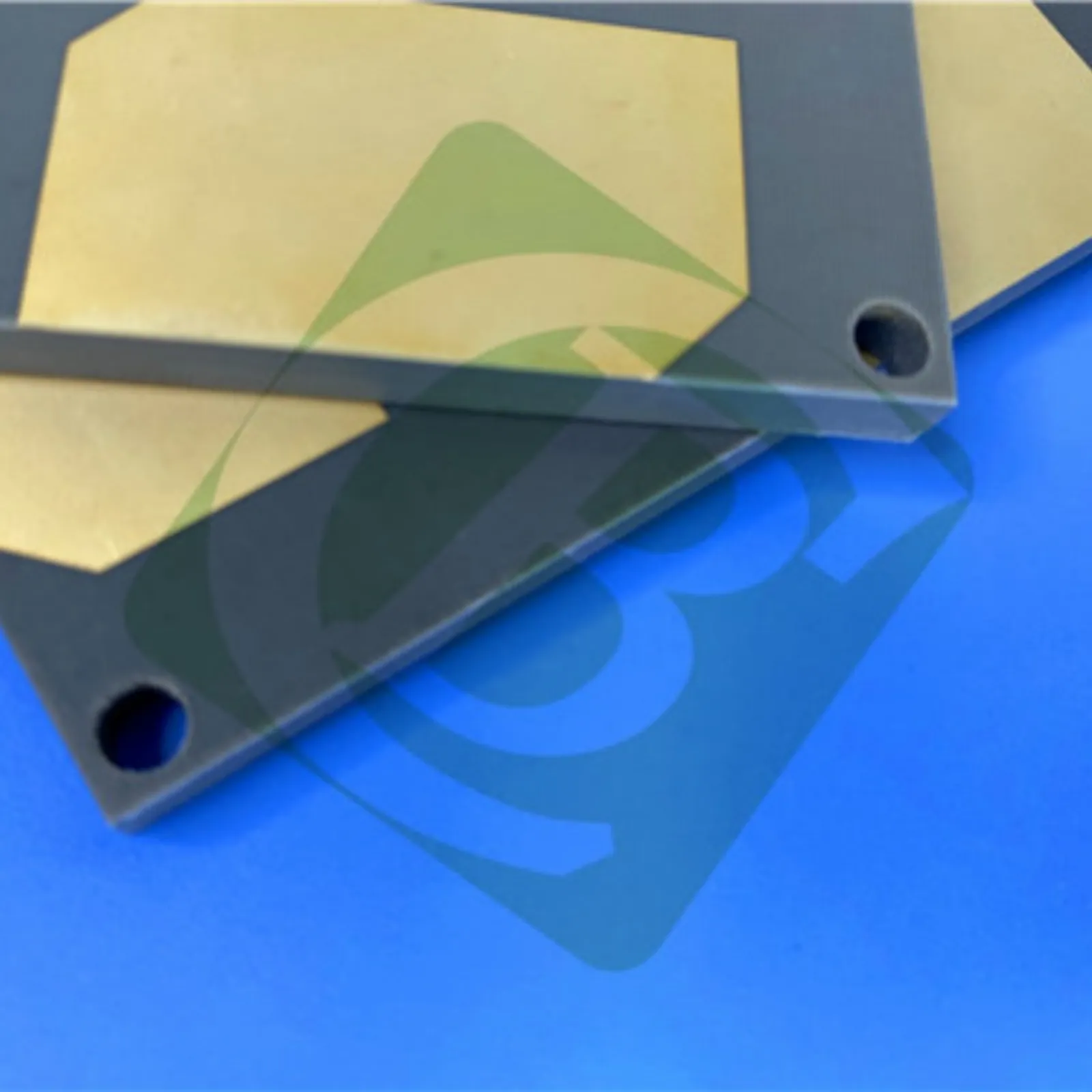 | Wangling F4BM217 LaminateDK 2.17Df 0.001 | ||||
| Wangling F4BME217 LaminateDK 2.17Df 0.001 | ||||
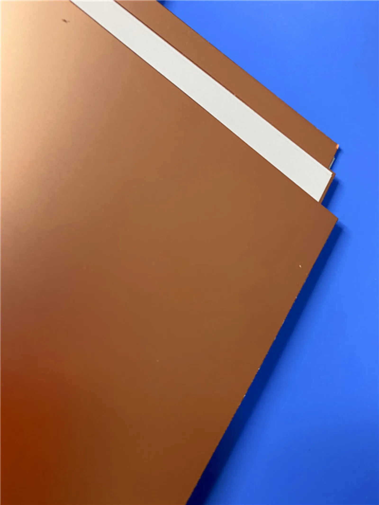 | Rogers IsoClad 917 LaminateDK 2.17Df 0.0013 | ||||
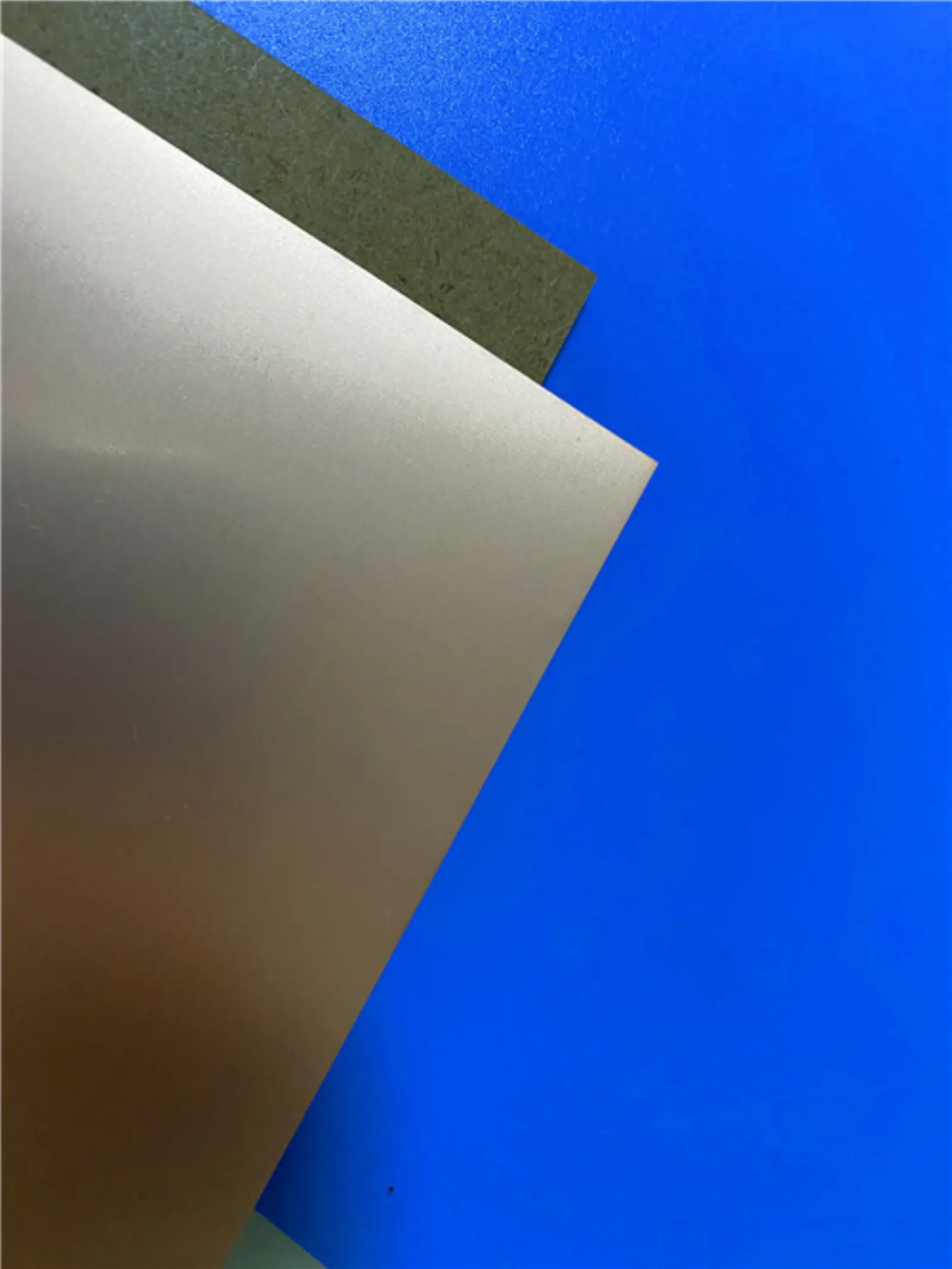 | Wangling F4BM220 LaminateDK 2.20Df 0.001 | ||||
 | Wangling F4BME220 LaminateDK 2.20Df 0.001 | ||||
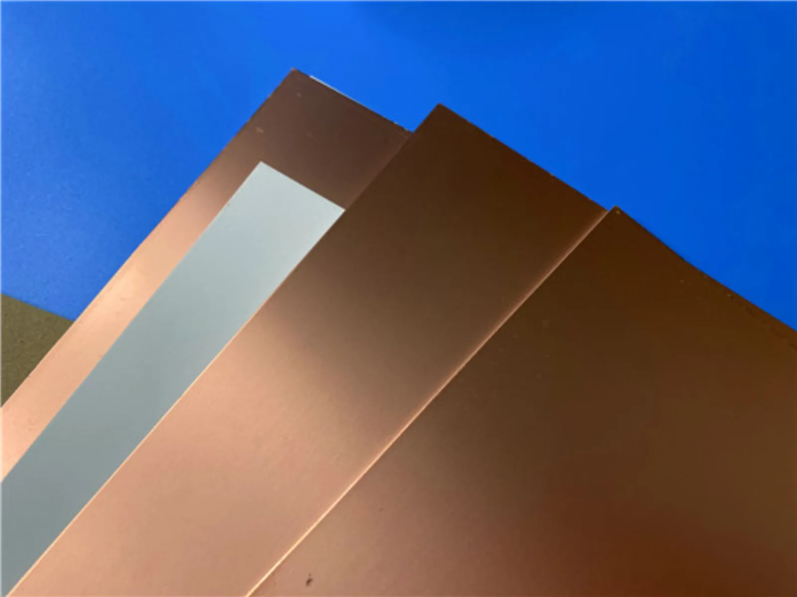 | Wangling F4BTMS220 LaminateDK 2.20Df 0.0009 | ||||
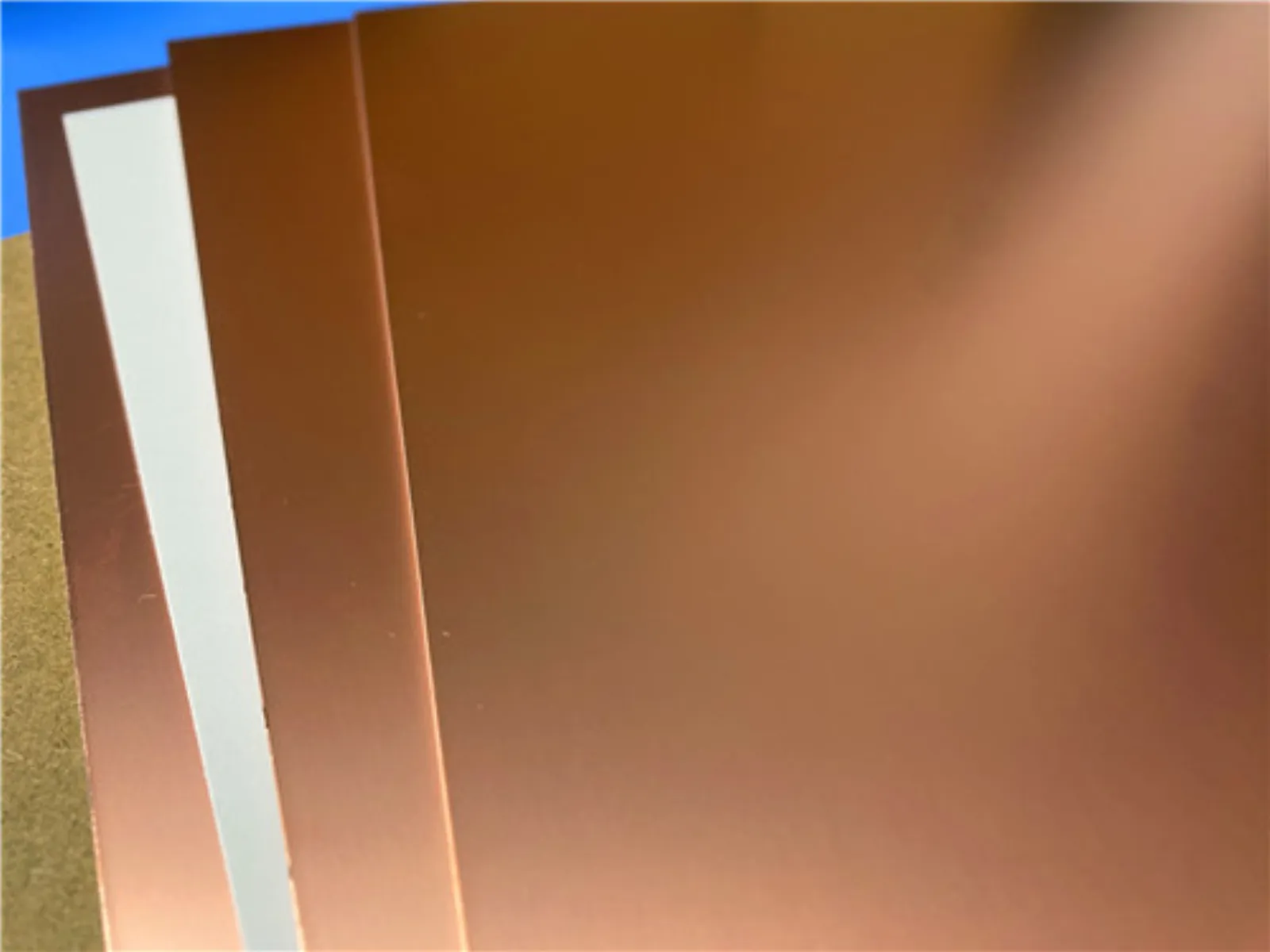 | Taconic TLY-5 LaminateDK 2.20Df 0.0009 |
Material selection notes
Low DK LAMINATES 2.17-3.9
Substrate selection is decisive for high-frequency PCB performance. Total loss combines conductor loss, driven by copper surface roughness and operating frequency, with dielectric loss, set by the material's dissipation factor (Df); open-structure layouts also radiate, and excessive radiation wastes power and causes crosstalk to adjacent traces. Lower Dk increases radiation and lengthens the guided wavelength, requiring larger layouts for the same electrical length, while higher Dk confines the electromagnetic field and shrinks circuit dimensions. The right Dk-Df combination therefore has to balance loss, radiation, size and coupling for each application.
Low DK LAMINATES 2.0-3.9
Discover our range of Copper Clad Laminates, renowned for their robust electrical insulation and versatile performance, making them fundamental to reliable PCB fabrication.