
PCB Industry Terminology and Definitions - HDI (High-Density Interconnect)
Published Jul 21, 2025
HDI (High-Density Interconnect)
HDI, an abbreviation for High-Density Interconnector, represents an advanced technology in printed circuit board (PCB) manufacturing.
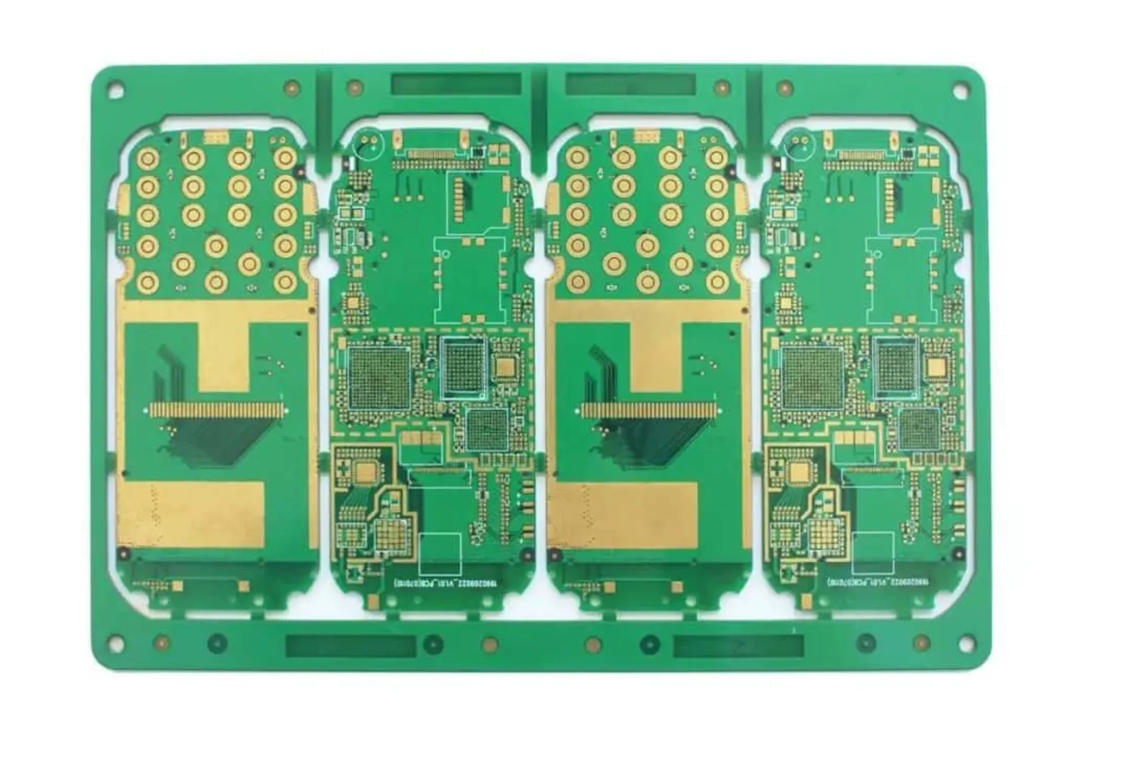
HDI Boards
These are high-density circuit boards utilizing micro-blind and buried via technology, specifically designed as compact solutions for space-constrained applications.
Manufacturing Process
HDI boards are typically produced using sequential lamination (build-up) technology. The technical sophistication increases with additional build-up layers:
Standard HDI: 1 build-up layer
Advanced HDI: 2+ build-up layers, incorporating sophisticated PCB technologies like:
Stacked vias
Plated filled vias
Laser direct drilling
Technical Advantages
For PCBs exceeding 8 layers, HDI technology offers:
Lower production costs compared to traditional complex lamination processes
Superior electrical performance and signal integrity
Enhanced capabilities for advanced packaging technologies
Improved performance in:
RF interference suppression
EMI reduction
ESD protection
Thermal management
HDI vs Conventional PCBs
| Characteristic | Conventional PCB | HDI PCB | |
| Base Material | FR-4 (epoxy resin + e-glass) | Specialized low-glass/no-glass substrates | |
| Drilling Technology | Mechanical drilling | Advanced laser drilling | |
| Layer Density | Standard density | Ultra-high density | |
| Cost Efficiency | Economical for simple designs | Optimized for complex, high-density designs | |
Material Note:
While traditional HDI required glass-free bonded copper foil due to laser drilling limitations, modern high-power laser systems can now penetrate 1180-grade glass fabric, eliminating this material distinction in many applications.