
How Are RO3210 Hybrid PCB Made with Immersion Silver+Gold and a Depth-Controlled Slot?
Published Sep 30, 2026
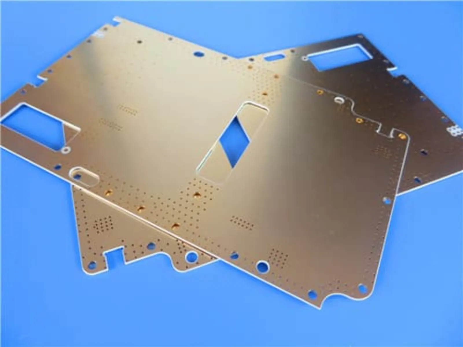
In microwave, RF, radar, and phased array applications, PCBs often have to withstand high-frequency loss while also supporting embedded components, 3D packaging, and long-term reliability in harsh environments. The **RO3210 + RO4450F hybrid 4-layer board**.html) is a high-performance solution designed for exactly these needs: it uses Rogers RO3210 ceramic-filled PTFE material as the core dielectric, bonding two 0.508mm RO3210 cores together with a single sheet of 0.2mm RO4450F prepreg in a symmetrical 4-layer hybrid structure. The finished board is approximately 1.22mm thick, with 1oz copper on all four layers, an immersion silver + gold surface finish, and a depth-controlled slot.
1. Material Selection: RO3210 and RO4450F Prepreg
RO3210 is a ceramic-filled PTFE composite laminate with a dielectric constant (Dk) of 10.2 ± 0.30 at 10GHz and a dissipation factor (Df) of only 0.0022. Its thermal coefficient of dielectric constant is -395 ppm/°C, thermal conductivity is 0.95 W/m/K, decomposition temperature (Td) is as high as 500°C, moisture absorption is only 0.05%, and it is compatible with lead-free processes with a UL 94 V-0 flammability rating. These characteristics allow it to maintain stable electrical performance at high frequencies while also providing good heat dissipation and dimensional stability.
The RO4450F prepreg is the key bonding layer in this hybrid structure. Its nominal thickness is 0.2mm, which provides sufficient resin to bond the RO3210 cores while maintaining a low-profile bond line. Unlike thin, low-flow prepregs such as 1080, RO4450F is a high-performance, low-flow material that requires lamination parameters optimized for the RO3210 surface to ensure reliable resin flow, fill, and interlayer bonding.
2. Stackup Design: Symmetry Is Key
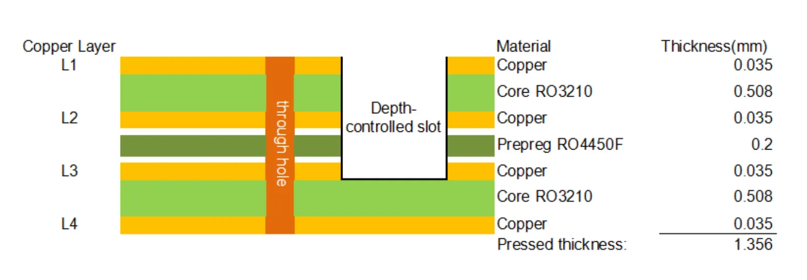
The layer sequence of this 4-layer board is:
L1: Copper, 35μm (1oz)
Dielectric: RO3210 core, 0.508mm, Dk 10.2 ± 0.30 @ 10GHz
L2: Copper, 35μm (1oz)
Prepreg: RO4450F, 0.2mm
L3: Copper, 35μm (1oz)
Dielectric: RO3210 core, 0.508mm, Dk 10.2 ± 0.30 @ 10GHz
L4: Copper, 35μm (1oz)
The total dielectric thickness is 0.508 + 0.2 + 0.508 = 1.216mm. Adding four layers of 1oz copper (4 × 0.035mm = 0.14mm), the nominal finished thickness is approximately 1.356mm, which is rounded to a pressed thickness of 1.22mm in the specification.
This symmetrical 0.508 + 0.2 + 0.508mm structure is the core design for controlling warpage. The neutral axis is located at the center of the RO4450F prepreg, and the RO3210 cores on both sides are identical in thickness and material properties. Therefore, thermal expansion is balanced on both sides of the center, effectively preventing the board from bowing or twisting during thermal cycling. At the same time, the RO4450F prepreg minimizes the volume proportion of low-CTE material while ensuring bonding strength, thereby reducing the impact of CTE mismatch.
3. Manufacturing Process: The Challenges Lie in Bonding, Fill, Warpage Control, Immersion Silver + Gold, and the Depth-Controlled Slot
The hybrid lamination of RO3210 and RO4450F presents several main process challenges:
First, PTFE surface bonding. The surface energy of RO3210 is very low, so surface treatment such as sodium etching is required to allow the RO4450F prepreg to achieve sufficient peel strength. Otherwise, even if the stackup design is reasonable, delamination may occur during subsequent thermal cycling.
Second, resin flow and fill. The RO4450F prepreg requires resin flow characteristics optimized for the RO3210 surface to ensure it completely fills larger etched areas on the inner layers and avoids voids. At the same time, it must fill the gaps between the RO3210 cores and the copper features, preventing delamination and ensuring reliable electrical performance.
Third, CTE mismatch and residual stress. The X/Y CTE of RO3210 is 13/11 ppm/°C, and its Z-axis CTE is 16 ppm/°C, which differs somewhat from RO4450F, making stress likely at the interface. A symmetrical stackup can balance the stress on both sides, but the cooling process after lamination still needs to be controlled to reduce residual stress. In addition, the dimensional stability of RO3210 is -0.35/-0.31 mm/m, and this shrinkage must be taken into account when designing the artwork.
Fourth, the immersion silver + gold surface finish. This board uses a combined immersion silver and gold process, combining the advantages of both surface finishes. Immersion silver provides excellent solderability and high conductivity, and its low insertion loss is particularly suitable for high-frequency signal transmission. However, the silver layer may tarnish over time, so immersion gold is combined with it to enhance long-term reliability. Immersion gold provides excellent corrosion resistance, wire bondability, and long-term stability. The gold layer is inert and does not oxidize, making it suitable for applications requiring long shelf life and reliable performance in harsh environments. The combination retains the low loss and solderability of silver while gaining the corrosion resistance and reliability of gold, making it particularly suitable for RF and microwave applications with critical signal integrity and long-term reliability requirements.
Fifth, the depth-controlled slot. A depth-controlled slot (also known as a depth-controlled cavity or blind slot) is a feature milled from the top surface of the PCB to a specific depth, stopping at a designated layer. Unlike a through-hole or a standard slot, it does not penetrate the entire board thickness. Its depth is typically controlled within tight tolerances (for example, ±0.05mm or better) to ensure it stops at the target layer. Its main functions include: providing cavities for embedded active or passive components such as filters and MMICs, reducing the overall height of the module; providing recessed areas for interface components such as edge-launch connectors, ensuring precise alignment and reliable connections; enabling 3D packaging by allowing components to be placed within the board thickness, saving valuable surface area; improving heat dissipation by exposing inner layer copper planes for heat spreading or attaching heat sinks; and in RF applications, creating air-filled cavities that reduce dielectric loss and improve signal integrity. In this PCB, the depth-controlled slot is designed to expose the inner layers (L2–L3) for specific functional requirements such as component mounting or signal routing, while maintaining the mechanical integrity and electrical performance of the board.
4. Electrical and Thermal Performance: The Foundation for High-Frequency Applications
The high Dk of RO3210 (10.2) means that at the same frequency, circuit dimensions can be significantly reduced, which is very beneficial for the miniaturization of microwave and phased array modules. The low Df (0.0022 @ 10GHz) ensures extremely low signal loss, making it suitable for radar, filters, microstrip patch antennas, VCOs, satellite communications, and base station antennas. Its thermal conductivity of 0.95 W/m/K, combined with a decomposition temperature of 500°C, provides good thermal management capability in high-power scenarios. The X/Y CTE of 13/11 ppm/°C is relatively close to that of copper, which also helps ensure the reliability of plated through holes.
5. Application Scenarios and Quality Assurance
This hybrid board is mainly aimed at high-frequency scenarios such as microwave, RF, radar systems, phased array antennas, band pass filters, microstrip patch antennas, voltage-controlled oscillators, satellite communications, base station antennas, and embedded component modules. On the manufacturing side, it is produced in accordance with IPC-6012 Class 3 standards, with 100% electrical testing before shipment. The facility is ISO 9001:2015 and UL certified, supports Gerber RS-274-X files, and ships worldwide.
Summary
The design essence of the RO3210 + RO4450F hybrid 4-layer board can be summed up in one sentence: use a symmetrical stackup to "hold down" the CTE mismatch between the two materials, use RO4450F prepreg to make the bond line reliable, use the high Dk and low Df of RO3210 to "max out" high-frequency performance, and then use immersion silver + gold and the depth-controlled slot to "raise" reliability and 3D integration capability. In manufacturing, the key focuses are PTFE surface treatment, resin flow and fill of the RO4450F prepreg, stress control during lamination cooling, process matching of immersion silver and gold, and depth accuracy of the depth-controlled slot. As long as these hurdles are managed, this 1.22mm thick hybrid board can achieve a balance of thinness, low loss, embedding capability, and long-term reliability in microwave, radar, and phased array applications.