
不同产品领域该选哪种电路板?
发布于 2025-11-07
This article systematically outlines the key points for PCB material selection, process design, performance indicators, and cost control across six typical application scenarios, supplemented with a pitfall guide, aiming to provide engineers with a one-stop practical reference.
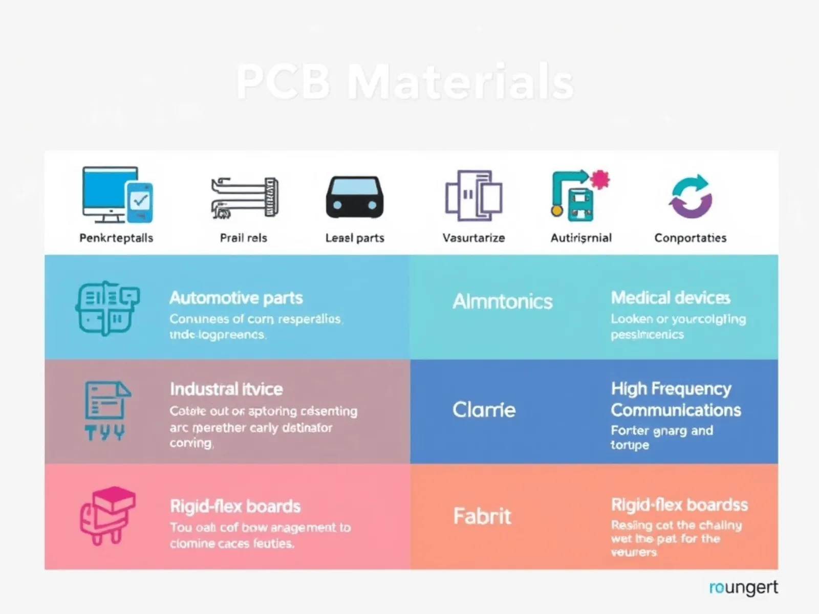
I. Consumer Electronics: Balancing Thinness/Lightness and High Integration
Core Needs: Miniaturization, low power consumption, cost sensitivity.
Typical Applications: Mobile phones, laptops, TWS earphones, smartwatches.
1. Material Selection
Substrates:
FR-4 (Tg 130°C): Mainstream choice, low cost (~¥150/m²), supports 4-6 layers, suitable for ordinary signal transmission (e.g., charging modules, key circuits).
High-Frequency Modified FR-4 (e.g., Shengyi S1141H): Dk=4.2, cost ~40% lower than Rogers, suitable for 1-6GHz signals (e.g., Wi-Fi 6 modules).
Polyimide (PI): Used for Flexible PCBs (FPC), thickness 0.025-0.1mm, withstands over 100,000 bends, adaptable for folding screen hinges.
Copper Foil:
1oz (35μm): Balances signal transmission and cost, suitable for most consumer electronics.
Ultra-thin Copper Foil (9-12μm): Reduces thickness, used in ultra-thin laptops (e.g., MacBook Air motherboard thickness 1.5mm).
2. Process Selection
HDI Technology: 1st/2nd order buried vias; line width/spacing 30/30μm, supports multi-chip integration (e.g., mobile phone motherboards integrating CPU, baseband).
Laser Drilling: Minimum aperture 0.1mm, increases wiring density (e.g., TWS earphone charging case PCB area reduced by 30%).
Surface Tratement:
HASL (Lead-Free): Low cost, good solderability, suitable for non-high-frequency areas (e.g., power interfaces).
ENIG: High surface flatness (Ra < 0.1μm), suitable for high-frequency signals (e.g., 5G RF antennas).
3. Performance Indicators
Thickness: 0.4-1.6mm, mobile phone motherboards typically use 0.8mm thin board + buried via design.
Impedance Control: Differential pairs (e.g., USB4.0) impedance 100Ω±10%, single-ended lines (e.g., GPIO) 50Ω±10%.
Thermal Design: Embedded copper blocks (thickness 0.5mm) or thermal conductive adhesive bonding, reduces SoC junction temperature (e.g., iPhone 15 Pro motherboard reduces A17 chip temperature by 10°C via embedded copper block).
4. Certifications and Reliability
Certifications: UL 94V-0 flame retardant certification, RoHS environmental certification.
Testing: High/low temperature cycling (-20°C~70°C, 500 cycles), drop test (1.2m height, 1 time on each of 6 sides).
5. Cost and Mass Production Advice
Cost Range: Single-layer board ¥50-100/m², 6-layer HDI board ¥800-1200/m².
Mass Production Optimization: Use panelization design (e.g., 8-up panel), reduces material waste (utilization rate increased to 90%).
II. Automotive Electronics: High Reliability and Extreme Environment Adaptation
Core Needs: Wide-temperature tolerance, vibration resistance, functional safety.
Typical Applications: BMS, Autonomous Driving Domain Controllers, Vehicle Radar.
1. Material Selection
Substrates:
High Tg FR-4 (Tg≥170°C): Suitable for engine compartments (-40°C~150°C), flexural strength 30% higher than ordinary FR-4.
Aluminum Substrate: Thermal conductivity 2.0 W/m·K, used for motor controllers, improves heat dissipation efficiency by 50%.
Polyimide (PI): Used in high-temperature areas (e.g., near turbochargers), short-term tolerance 200°C.
Copper Foil: 3-6oz (105-210μm): High current transmission (50-200A), reduces line resistance (e.g., BMS busbar design).
2. Process Selection
Heavy Copper Plating: Hole wall copper thickness ≥25μm, improves vibration resistance (<3% resistance change after 1 million vibrations).
Composite Surface Treatment: Electroless Nickel Immersion Gold (ENIG) + Immersion Tin, reduces solder joint corrosion area by 80% after salt spray test (1000 hours).
Conformal Coating: Thickness 25-50μm, resistant to oil, salt spray, complies with ISO 16750 standard.
3. Performance Indicators
Temperature Range: -40°C~150°C, supports 1000 temperature cycles (-40°C~125°C).
Vibration Resistance: 20G acceleration, 10-2000Hz random vibration, requires continuous inspection of solder joint void rate <5%.
Functional Safety: Complies with ISO 26262 ASIL B-D levels, key signal dual-path redundancy design (e.g., sensor interfaces in autonomous driving domain controllers).
4. Certifications and Reliability
Certifications: IATF 16949 Quality Management System, AEC-Q100 (passive components), AEC-Q200 (active components).
Testing:
High Voltage Test: 800V platform requires CAF test (1000V DC, no conductive anodic filament).
EMC Test: Radiated interference ≤30dBμV/m (30-1000MHz), complies with CISPR 25 standard.
5. Cost and Mass Production Advice
Cost Range: Single-layer board ¥300-500/m², 16-layer HDI board ¥3000-5000/m².
Mass Production Optimization: Adopt modular design (e.g., separate BMS cell detection board and main control board), reduces maintenance costs (failure rate decreased by 50%).
III. Medical Devices: High Precision and Biocompatibility
Core Needs: Zero tolerance, sterilization resistance, biosafety.
Typical Applications: CT Scanners, Pacemakers, Wearable Monitors.
1. Material Selection
Substrates:
Halogen-Free FR-4 (Cl/Br < 900ppm): e.g., Isola FR406, UL 94 V-0 certified, avoids drug solution contamination.
Polyimide (PI): For implantable devices, biocompatibility test cell survival rate ≥98%, resistant to EO sterilization (50°C, 12 hours). Surface Treatment:
ENIG (Au≥0.1μm): Excellent solderability, suitable for precision soldering (e.g., pacemaker electrode interfaces).
Medical Grade Conformal Coating: e.g., Dow Corning TC-5288, withstands 1000 alcohol wipes, water absorption <0.01%.
2. Process Selection
Laser Drilling: Minimum aperture 0.15mm, supports high-density wiring (e.g., CT detector pixel arrays).
Aseptic Packaging: Titanium alloy shell + laser welding, hermeticity test leakage rate < 1×10⁻⁵ mbar·L/s.
3. Performance Indicators
Signal Accuracy: ADC sampling error ≤±0.5LSB, noise control <15μV (e.g., ultrasound echo signal processing).
Insulation Performance: High-voltage areas (e.g., MRI gradient coils) spacing ≥0.5mm, insulation resistance >10¹²Ω.
4. Certifications and Reliability
Certifications: ISO 13485 Quality Management System, FDA 510(k) (non-implantable), CE MDR (implantable).
Testing:
Biocompatibility: Full set of ISO 10993 tests (cytotoxicity, sensitization), implantable devices require genetic toxicity testing.
Sterilization Resistance: After ethylene oxide sterilization, Tg value decrease <10%, interlayer bonding strength maintained ≥1.2N/mm.
5. Cost and Mass Production Advice
Cost Range: Single-layer board ¥800-1500/m², 8-layer board ¥5000-8000/m².
Mass Production Optimization: Establish material traceability files; select suppliers with Class 1000 cleanrooms, dust particle control ≤0.5μm.
IV. Industrial Control: Long-Term Stability and Anti-Interference
Core Needs: Vibration resistance, EMI resistance, wide-temperature operation.
Typical Applications: PLC Controllers, Industrial Robots, Sensor Nodes.
1. Material Selection
Substrates:
High Tg FR-4 (Tg≥170°C): Suitable for high-temperature environments (-40°C~125°C), flexural strength 20% higher than ordinary FR-4.
Ceramic Substrate: Thermal conductivity 25 W/m·K, used for high-power modules (e.g., frequency converter IGBT heat dissipation).
Copper Foil: 2oz (70μm): High current transmission (20-50A), reduces trace temperature rise (e.g., motor drive circuits).
2. Process Selection
Heavy Copper Plating: Hole wall copper thickness ≥25μm, improves vibration resistance by 50% (<5% resistance change after 1 million vibrations).
3W Spacing Rule: Critical signal line spacing ≥3x line width, reduces crosstalk (e.g., Industrial Ethernet differential pairs).
3. Performance Indicators
Temperature Range: -40°C~125°C, supports 1000 hours 85/85 test (85°C/85%RH).
Vibration Resistance: 10-2000Hz random vibration, acceleration 20G, component fixation uses red glue (coverage area ≥80%).
4. Certifications and Reliability
Certifications: IEC 61131-2 (Industrial control standard), UL 94 V-0 flame retardant certification.
Testing:
Salt Spray Test: 5% NaCl solution, 35°C, 1000 hours, solder joint corrosion area <5%.
EMC Test: Conducted interference ≤40dBμV (150kHz-30MHz), complies with CISPR 32 standard.
5. Cost and Mass Production Advice
Cost Range: Single-layer board ¥200-350/m², 4-layer board ¥1000-1500/m².
Mass Production Optimization: Adopt modular design (e.g., separate PLC I/O modules), reduces maintenance cost by 40%. Select certified suppliers, stable lead time of 10-15 days.
V. High-Frequency Communication: The Ultimate Pursuit of Signal Integrity
Core Needs: Low loss, stable impedance, high-frequency response.
Typical Applications: 5G Base Stations, Satellite Communication, Millimeter-Wave Radar.
1. Material Selection
Substrates:
Rogers RO4350B: Dk=3.48±0.05, Df=0.0037@10GHz, suitable for signals above 24GHz (e.g., vehicle radar).
Shengyi S1000-2M: Dk=3.0±0.05, Df=0.0027@10GHz, cost ~50% lower than Rogers, suitable for 5G base station AAU modules.
Copper Foil: VLP Copper Foil (Surface Roughness Ra < 0.5μm): Reduces high-frequency loss (e.g., 5G RF line loss reduced by 0.5dB/10cm).
2. Process Selection
mSAP: Line width/spacing 3.5/3.5mil (90/90μm), supports high-density high-frequency routing (e.g., 64T64R mmWave radar).
Differential Pair Design: Impedance 100±5%, line width/spacing 4.5/5.5mil (115/140μm), for PCIe 5.0 interfaces.
3. Performance Indicators
Signal Loss: Insertion loss ≤0.3dB/cm @28GHz, return loss ≤-15dB.
Impedance Stability: Impedance variation ±3Ω over -40°C~125°C range, complies with IST test standard.
4. Certifications and Reliability
Certifications: IPC-6013 Class 3 (High Reliability), MIL-PRF-55110G (Military Standard).
Testing:
S-Parameter Test: S21 ≥ -10dB @20GHz, eye diagram extinction ratio ≥6dB (e.g., 5G NR signal).
Thermal Shock Test: -55°C~260°C, 1000 cycles, interlayer bonding strength ≥1.5N/mm.
5. Cost and Mass Production Advice
Cost Range: Single-layer board ¥1000-2000/m², 8-layer board ¥8000-12000/m².
Mass Production Optimization: Use step lamination process, reduces material stress (layer misalignment ≤50μm). Select suppliers with high-frequency testing capabilities, provide complete S-parameter report.
VI. Rigid-Flex Boards: Flexible Solutions for Dynamic Scenarios
Core Needs: Bend resistance, 3D topology, space optimization.
Typical Applications: Folding Screen Hinges, Industrial Robot Joints, Medical Endoscopes.
1. Material Selection
Flexible Layers:
Polyimide (PI): Thickness 0.025-0.1mm, withstands over 100,000 bends (radius≥1mm), adaptable for folding screens.
Liquid Crystal Polymer (LCP): Dk=2.95±0.02, used for high-frequency flexible cables (e.g., 5G phone antennas).
Rigid Layers: FR-4 (Tg≥150°C): Combined with flexible layers, supports multi-layer rigid-flex stacking (e.g., industrial robot control boards).
2. Process Selection
Adhesiveless Lamination (RCC): Reduces dielectric layer thickness (total thickness ≤0.2mm), impedance control accuracy ±5%, suitable for 77GHz radar.
Stress Relief Slots: Laser-cut V-shaped slots in bend areas (depth ≤50% board thickness), increases lifespan by 30%.
3. Performance Indicators
Bend Cycle Life: Over 100,000 cycles (IPC-6013D standard, 90° bend angle, 1mm radius).
Impedance Stability: Differential impedance variation ±5% after bending, suitable for high-speed signals (e.g., HDMI 2.1).
4. Certifications and Reliability
Certifications: IPC-2223C (Rigid-Flex Design Standard), UL 94 V-0 flame retardant certification.
Testing:
Dynamic Flex Test: 1 cycle/sec, <5% resistance change after 100,000 cycles, no insulation failure.
IP67 Waterproof: Coated with magnetic flux coating, no corrosion after 1000-hour salt spray test.
5. Cost and Mass Production Advice
Cost Range: 4-layer rigid-flex board ¥3000-5000/m², 8-layer rigid-flex board ¥8000-12000/m².
Mass Production Optimization: Use pre-bending process (e.g., 30° pre-bend for folding screen hinge) to reduce stress concentration in use.
Select suppliers with rigid-flex mass production experience, yield can reach over 85%.
VII. Pitfall Guide: Key Design Taboos and Selection Suggestions
1.[Consumer Electronics]: Avoid excessive layer count; strictly evaluate cost-effectiveness for HDI beyond 6 layers (e.g., 6-layer HDI often suffices for phone motherboards).
2.[Automotive Electronics]: Prohibit standard FR-4 in high-temperature areas (e.g., engine bay); must use higher temperature resistant PI substrate (Tg≥260°C) to ensure long-term reliability.
3.[Medical Devices]: Implantable PCBs must pass ISO 10993-12 (extractables testing) and strictly avoid halogen-containing materials to prevent biological toxicity risks.
4.[Industrial Control]: Avoid upright electrolytic capacitors in vibrating environments; prioritize horizontal installation reinforced with red glue to enhance mechanical stability.
5.[High-Frequency Communication]: For mmWave signals (>24GHz), use Rogers RO4350B or equivalent high-end materials; modified FR-4 cannot meet the extremely low loss requirements.
6.[Rigid-Flex Boards]: Strictly avoid placing vias in bend areas; prioritize blind vias or Laser Direct Imaging (LDI) processes to eliminate stress concentration points and ensure bend cycle life.