
什么是电路板走线开窗?
发布于 2026-05-15
PCB trace solder mask opening refers to removing the green solder mask (solder resist) from a portion of the PCB traces, exposing the copper underneath.
Steps:
- Open your PCB and select Top Layer
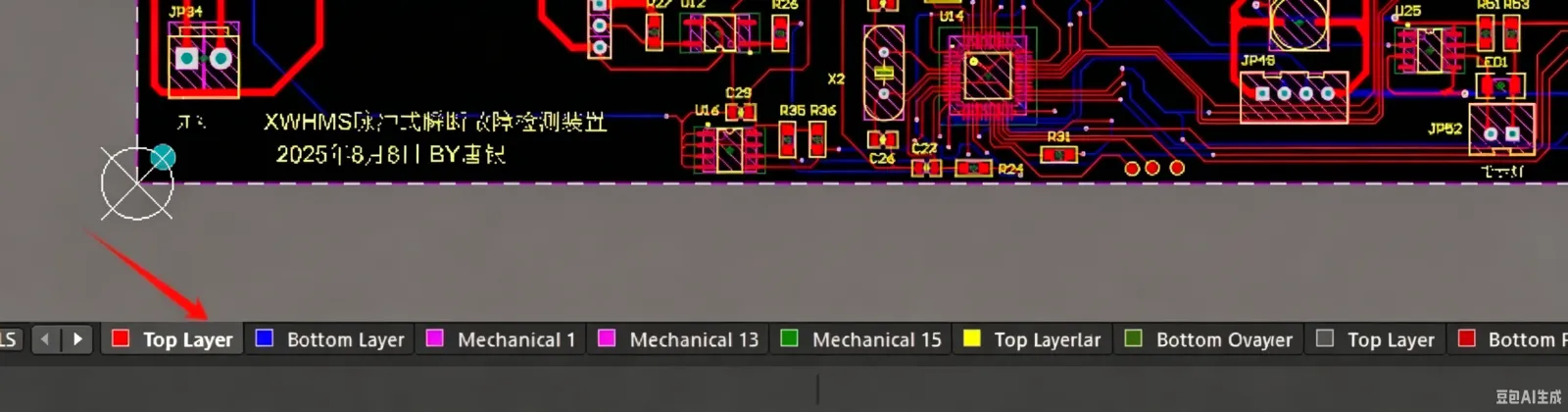
- Click on the Top Solder layer

- Select the line tool from the toolbar
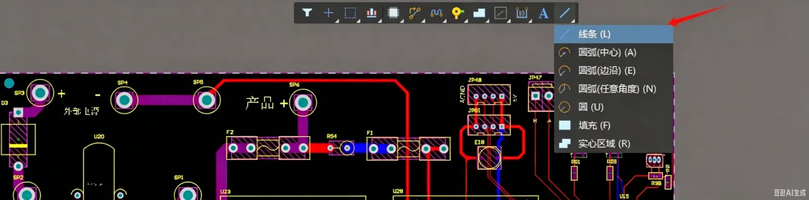
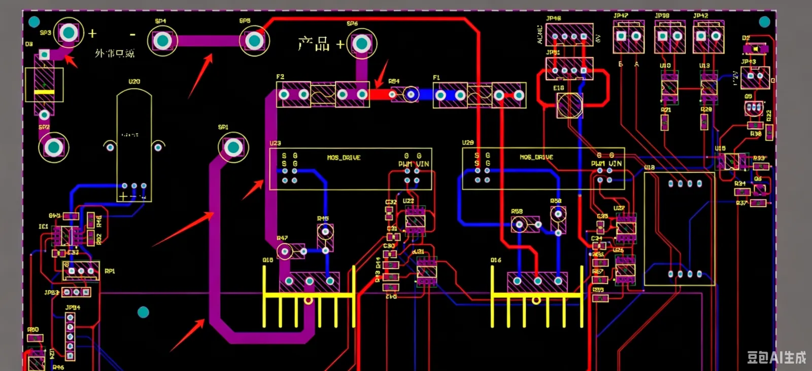
- Draw the line on the trace where you want to remove the green solder mask, as shown in the figure
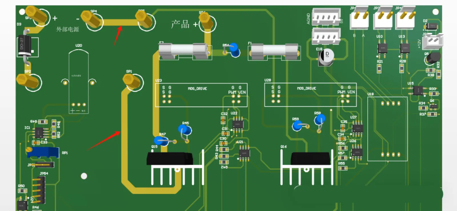
- Press "3" to switch to 3D view to see the actual effect – the green solder mask is removed and the copper is exposed
- For bottom layer solder mask opening, the process is similar – select Bottom Layer and then Bottom Solder layer