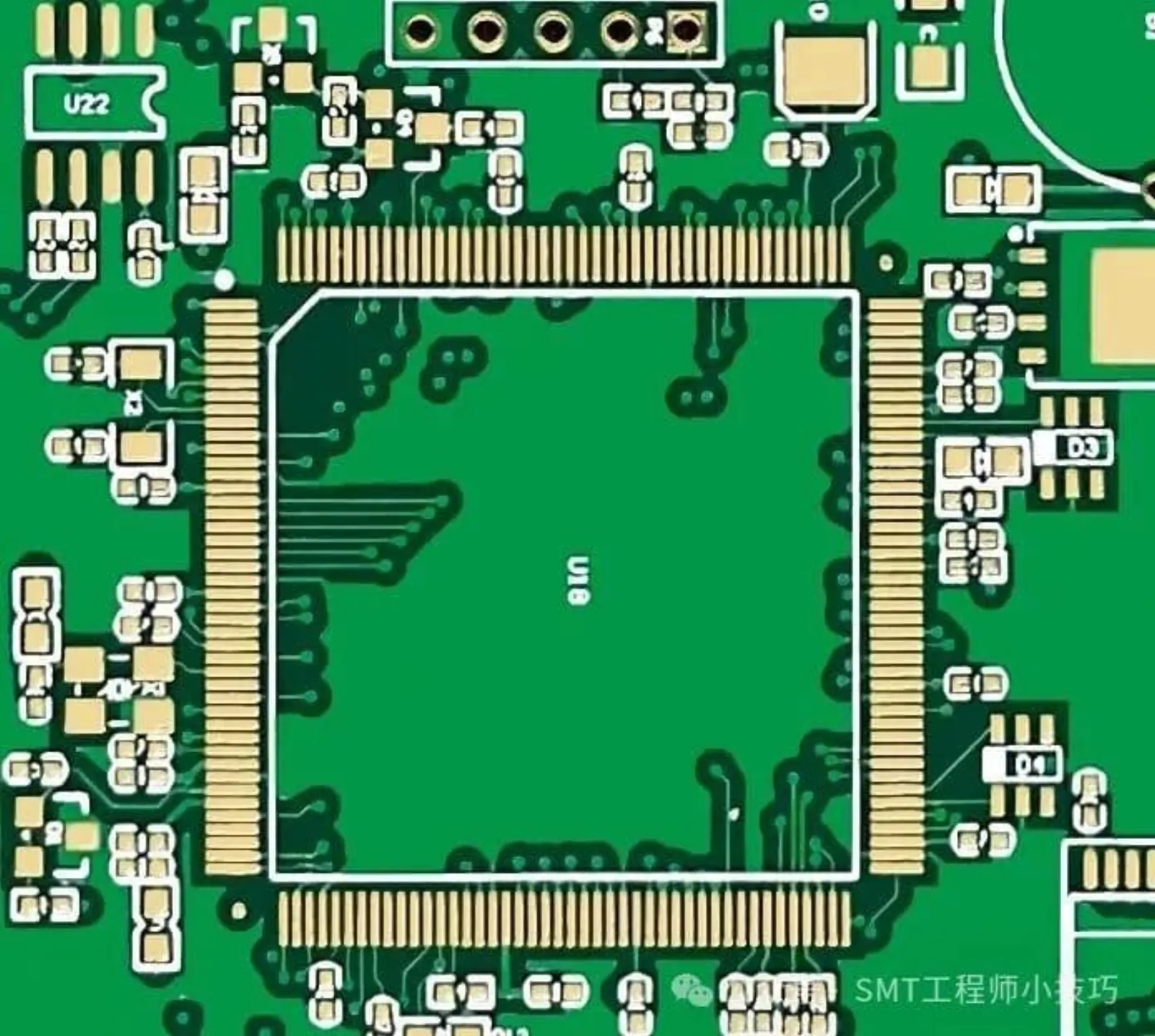
电路板表面处理工艺 — HASL / ENIG / OSP
发布于 2026-08-19
Hot Air Solder Leveling (HASL) (Process & Purpose)
Process: Pre-treatment → Flux application → Solder leveling → Solder leveling → Post-treatment
Purpose: 1. Protect the copper surface
2.Provide good solderability for subsequent assembly processes
Principle: Chemical reaction
Main raw material: Tin-lead bar
HASL (Pre-treatment)
Purpose: Remove organic contaminants and oxides from the copper surface.
Main chemical: SPS
Process key points: Copper ion concentration in the bath, temperature, line speed
HASL (Flux application)
Purpose: Facilitate solder adhesion to the copper surface.
Main raw material: 818 flux
Process key points: Viscosity and acidity of the flux; ease of cleaning
HASL (Solder leveling)
Purpose: Apply solder onto the copper surface.
Main raw material: Tin-lead bar (63/37)
Process key points:
A. Equipment performance
B. Air knife structure, angle, spray pressure, hot air temperature, solder pot temperature, board passing speed through the air knives, immersion time, etc.
HASL (Post-treatment)
Purpose: Wash off residual flux and oily residues carried out from the solder pot.
Electroless Nickel Immersion Gold (ENIG) (Process & Principle)
Process: Pre-treatment → Electroless nickel plating → Immersion gold → Post-treatment
Purpose:
- Flat solderable surface
2.Excellent electrical conductivity and oxidation resistance
Principle: Displacement reaction
Main raw material: Gold salt
ENIG (Pre-treatment)
Purpose: Remove excessive oxidation and minor impurities from the copper surface.
Main raw material: SPS (Sodium persulfate)
Process key points: A. Brush pressure B. SPS concentration C. Line speed
ENIG (Nickel/Gold Deposition – Purpose)
Electroless nickel/immersion gold stage
Purpose: Form a thin nickel-gold layer on the copper surface via displacement reaction (nickel thickness 3‑5µm, gold thickness 0.025~0.1µm)
Main raw material: Gold salt (Potassium Gold Cyanide, PGC)
Process key points:
A. Control of bath concentration and temperature
B. Rinsing water flow rate
C. Stability of the automatic dosing system
ENIG (Post-treatment)
Purpose: Rinse off residual chemicals from the gold surface to prevent gold oxidation
Main material: DI water
Process key points:
A. Water quality
B. Line speed
C. Drying temperature
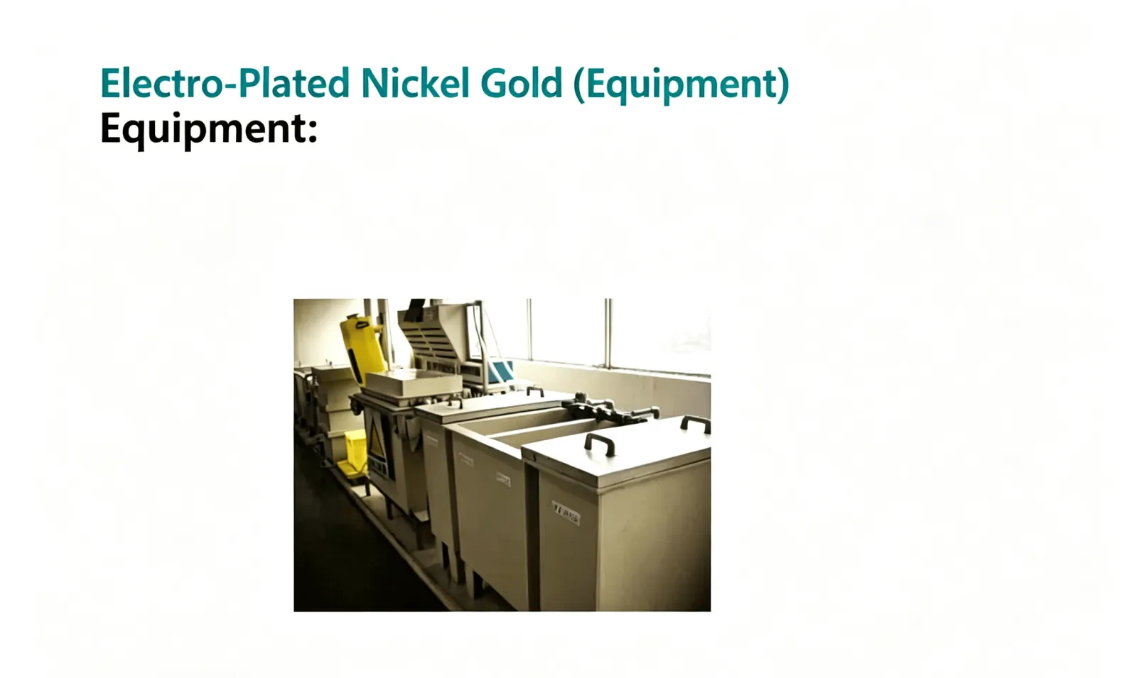
Electroplated Nickel Gold (Purpose)
Purpose: Deposit a nickel layer between the gold and copper as a barrier to prevent atomic interdiffusion between gold and copper over long-term use, which would expose the copper and affect contact performance; the main purpose of gold plating is to protect the copper surface from oxidation in air.
Main raw material: Gold salt
Process key points:
A. Control of bath concentration and temperature
B. Line speed control
C. Metallic contamination
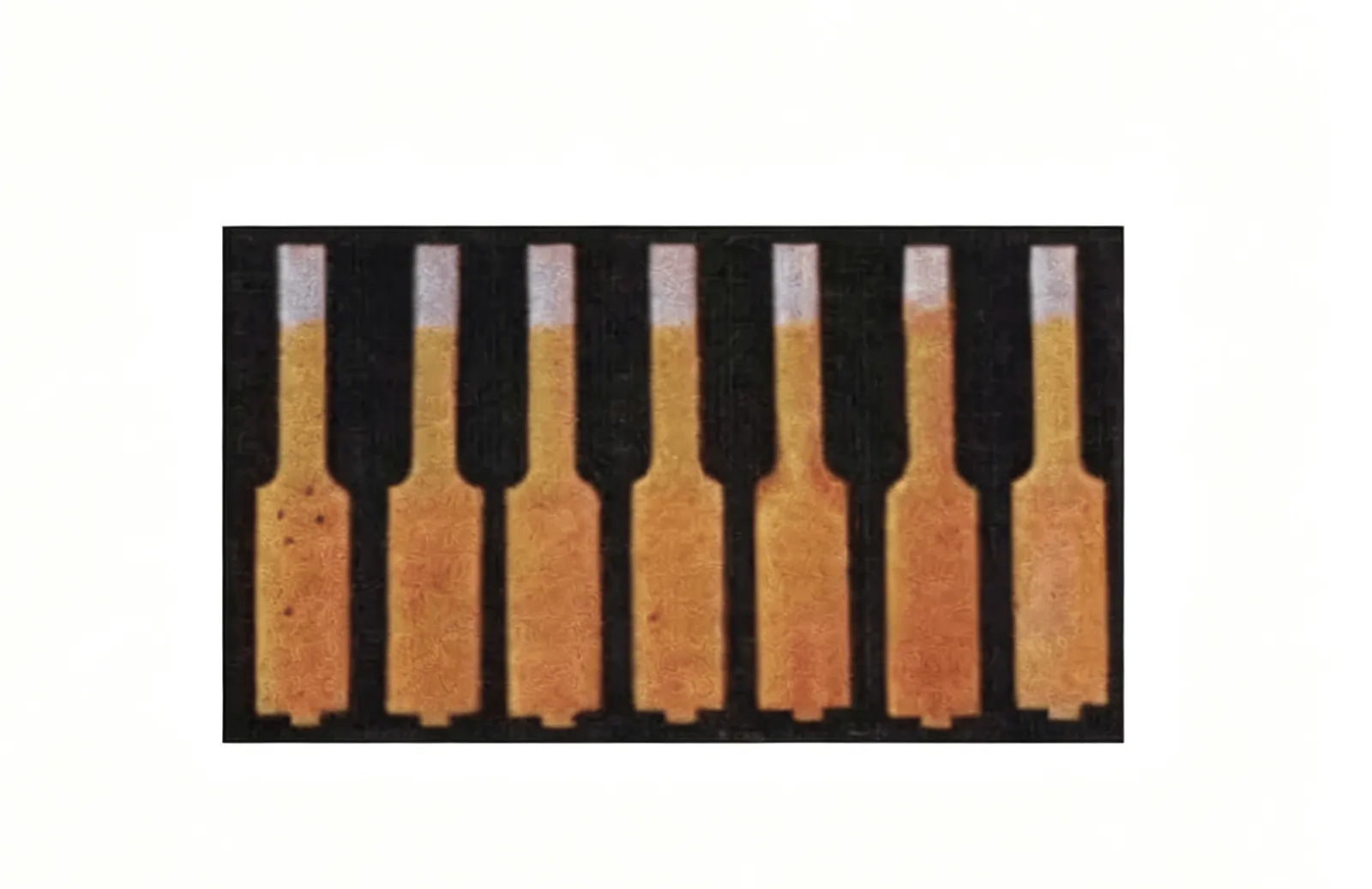
Gold Finger (G/F) (Process)
Purpose: Excellent electrical conductivity, oxidation resistance, and wear resistance
Principle: Redox reaction
Main raw material: Gold salt
Application Scenarios for Surface Finish Processes
- HASL process – Suitable for through-hole insertion (THT) devices, surface-mount resistors/capacitors/inductors, and SOP packages with a pitch of 0.5mm or above, where flatness requirements are not overly stringent.
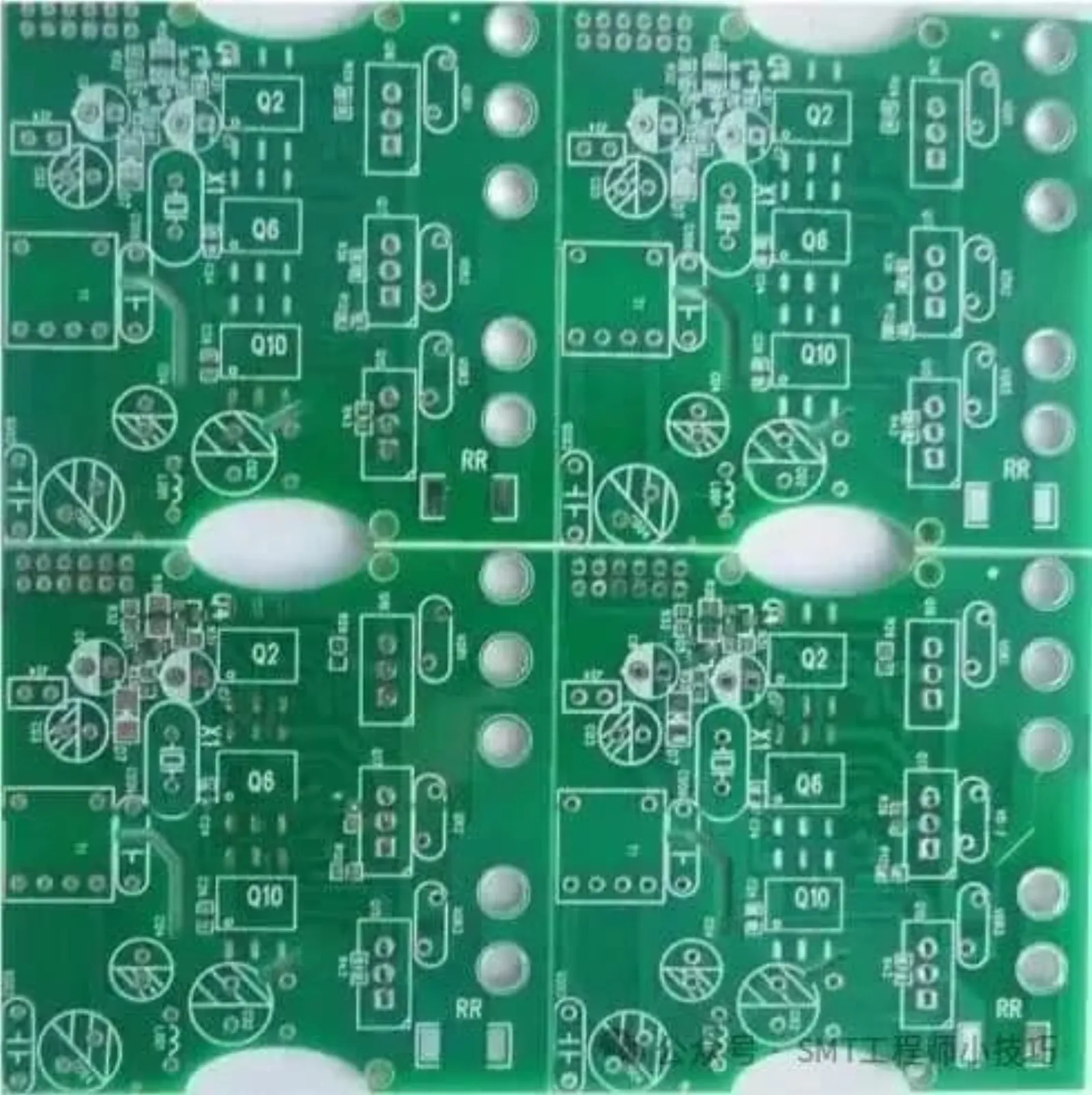
- OSP process – Short process flow, cost-effective…
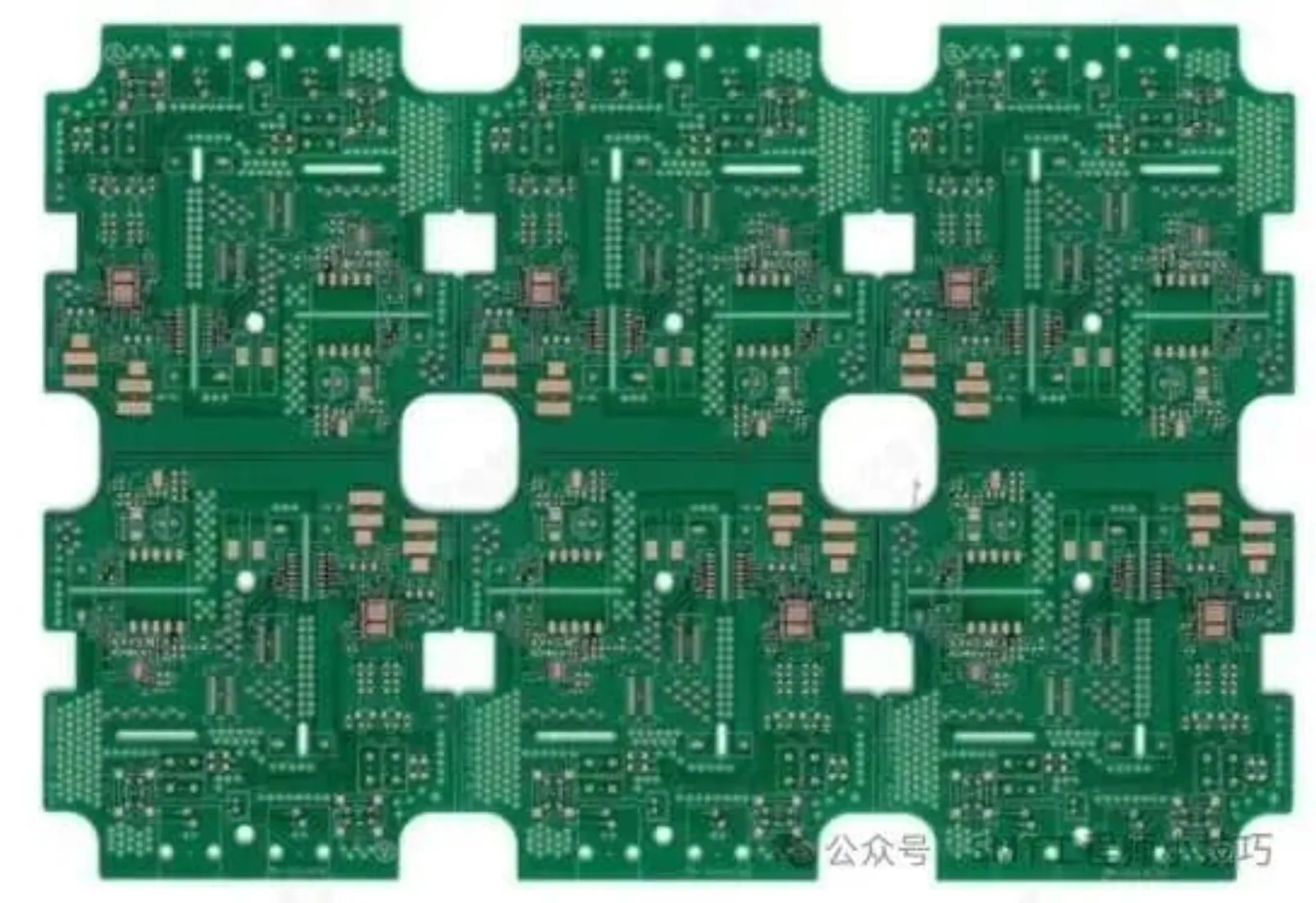
- ENIG process – Suitable for BGA, QFN, and QFP with a pitch below 0.4mm, for components requiring high surface flatness.